Supplementary figures
GPIO pads - management and user IO

GPIO pad structure - pads 0 (JTAG) and 1 (SDO)

GPIO pad structure - all pads except 0 and 1

Die arrangement and pads

Die voltage clamp arrangement

Die plot
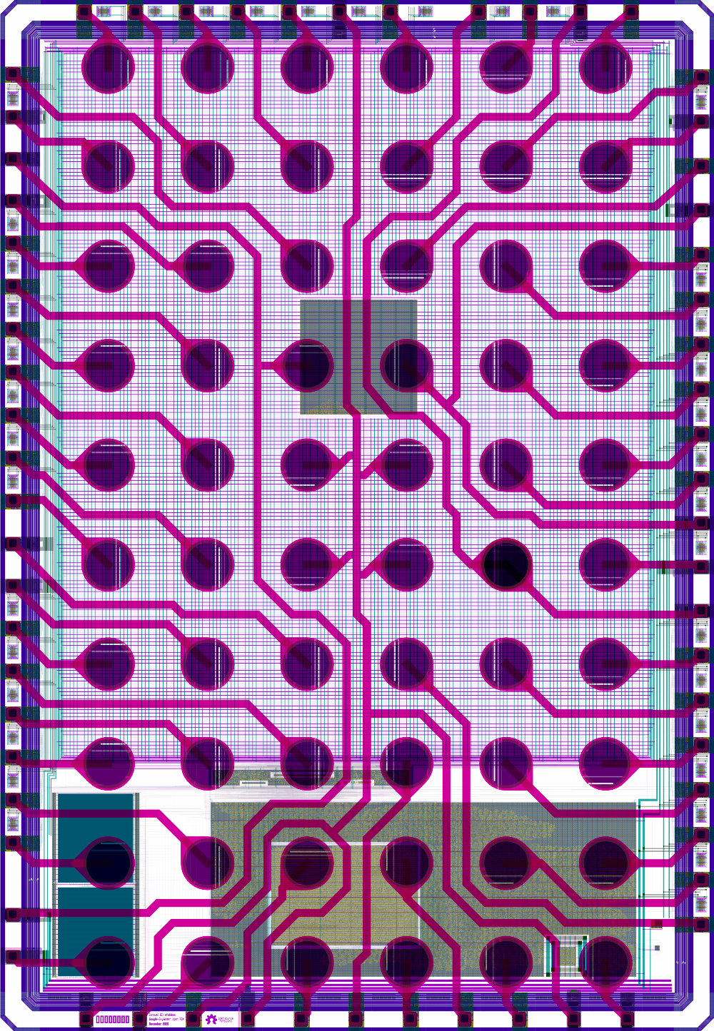
Die to WLCSP bond plan

Power domain splits

PCB example route pattern
